Planar Inductor Calculator
Design PCB spiral inductors online — free, instant, no sign-up. Enter your geometry and get inductance, Q-factor, DC resistance, self-resonant frequency, trace length, and resonant capacitor in one calculation. Supports square, hexagonal, octagonal, and circular spirals for NFC, RFID, RF filter, and power converter applications.
Reverse Designer (Target Inductance → Turns)
Solve the required number of turns (N) for a desired target inductance based on your current shape and size configurations.
NFC/RFID 13.56 MHz Tuning Assistant
Automatically tune your planar coil dimensions to the standard NFC frequency of 13.56 MHz, optimizing for a target antenna inductance of 2.0 µH.
Design Comparison Dashboard
Save and compare multiple spiral inductor geometries side-by-side to iterate on space, Q-factor, and performance.
| Design Name | Shape | Turns (N) | Outer (µm) | Inductance | Q-Factor | DCR (mΩ) | SRF (MHz) | Action |
|---|---|---|---|---|---|---|---|---|
| No saved geometries yet. Customize parameters and click "Save Geometry" to start comparing. | ||||||||
PCB Planar Inductor Calculator — Full Design Suite
This free online planar inductor calculator goes beyond basic inductance estimation. Enter your spiral geometry and get a complete design report: inductance, DC resistance, Q-factor at your operating frequency, self-resonant frequency, resonant tuning capacitor, trace length, fill ratio, and a live spiral preview — all calculated instantly using the Modified Wheeler Formula and Mohan expressions accurate to within 5% for standard PCB geometries.
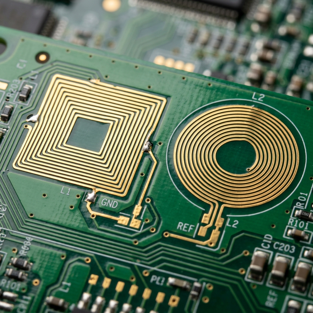
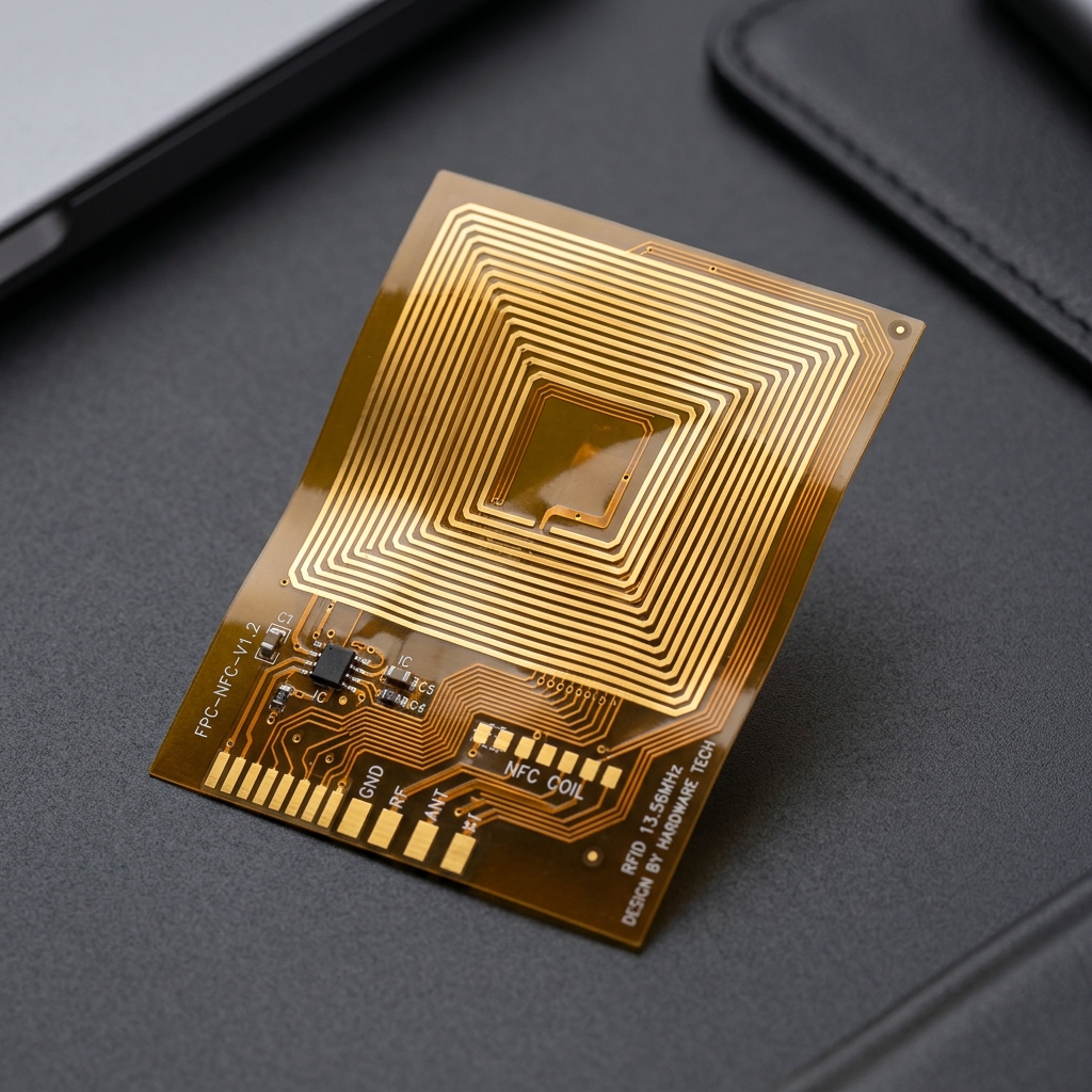
What Is a Planar Inductor?
A planar inductor (also called a PCB spiral inductor or flat spiral coil) is an inductive component formed by routing a copper trace in a spiral pattern directly onto the surface of a printed circuit board or silicon chip. Unlike traditional wire-wound inductors, there is no core and no wire — just the copper trace itself forming the coil.
This makes planar inductors ideal for any application where height is constrained or where the inductor must be integrated directly into the PCB stackup. They appear in NFC and RFID antennas, wireless charging coils, RF bandpass filters, impedance matching networks, and on-chip DC-DC converters.
What This Calculator Computes
Inductance (L) — nH or µH
The primary output. Calculated using shape-specific K₁ and K₂ constants in the
Modified Wheeler Formula: L ≈ K₁µ₀n²d_avg / (1 + K₂ρ).
Accuracy is within 5% of measured values for standard PCB trace geometries.
Inductance scales with the square of the number of turns —
doubling turns quadruples inductance.
DC Resistance (DCR) — mΩ
The total ohmic resistance of the copper spiral trace, calculated from the total trace length, trace width, copper thickness (based on selected copper weight), and copper resistivity (1.72 × 10⁻⁸ Ω·m). DCR is a key parameter for power loss estimation and Q-factor calculation. Thicker copper and wider traces both reduce DCR.
Q-Factor at Operating Frequency
The Quality Factor measures energy storage efficiency:
Q = (2π × f × L) / DCR.
Enter your target operating frequency and the tool calculates Q automatically.
Circular spirals achieve the highest Q because they minimize
trace length for a given inductance. Q degrades at higher frequencies due to
skin effect increasing effective resistance.
Self-Resonant Frequency (SRF) — MHz
The frequency at which parasitic inter-turn capacitance resonates with the inductance. Above the SRF the component behaves as a capacitor, not an inductor. The tool estimates SRF from the geometry and warns if your operating frequency is dangerously close. Rule of thumb: always operate below 30% of SRF.
Resonant Capacitor — pF
For LC tank circuits, RFID antennas, and RF filters, the tool calculates the
exact capacitor value needed to resonate at your target frequency:
C = 1 / (4π²f²L). For NFC at 13.56 MHz, this tells you the
tuning capacitor to hit resonance with your coil's calculated inductance.
Trace Length — mm
The total copper length of the spiral trace in millimeters, calculated from the geometry. Essential for PCB layout planning — know exactly how much copper your inductor uses before you start routing. Also feeds directly into the DCR and SRF calculations.
Inner Diameter & Fill Ratio
The inner diameter (D_in) is derived from the outer diameter, turns, trace width, and spacing. The fill ratio ρ = (D_out − D_in) / (D_out + D_in) describes how densely packed the spiral is. Optimal fill ratios are between 0.3–0.7 — too low wastes PCB area; too high reduces Q due to mutual flux cancellation from inner turns.
Live Spiral Preview (SVG)
A real-time SVG diagram renders the spiral to scale as you adjust parameters. Instantly verify the physical proportions of your design, compare shapes visually, and confirm the coil fits within your board's available area before committing to layout.
Inductance Formulas: Wheeler & Mohan
The calculator uses the Modified Wheeler Formula as the primary approximation, supplemented by the Mohan monomial expression for cross-validation on certain geometries.
Modified Wheeler: L ≈ K₁µ₀n²d_avg / (1 + K₂ρ)
Average Diameter: d_avg = (D_out + D_in) / 2
Fill Ratio: ρ = (D_out − D_in) / (D_out + D_in)
| Shape | K₁ | K₂ | Relative Q | PCB Ease |
|---|---|---|---|---|
| Square | 2.34 | 2.75 | Moderate | ★★★★★ Easiest |
| Hexagonal | 2.33 | 3.82 | Good | ★★★★☆ |
| Octagonal | 2.25 | 3.55 | Good | ★★★★☆ |
| Circular | 2.46 | 2.00 | Best | ★★★☆☆ Hardest |
Design Rules of Thumb
Geometry Guidelines
- Keep trace width (w) between 50–200 µm for RF applications; wider for power
- Set trace spacing (s) equal to trace width for best Q
- Target a fill ratio between 0.3–0.7 for optimal performance
- More turns → more inductance, but also more DCR and lower SRF
- Larger outer diameter → higher inductance for same number of turns
PCB Layout Rules
- Never place a ground plane under the coil — eddy currents kill inductance and Q
- Create a copper-free keepout zone on all layers beneath the spiral
- Use 45° mitered corners on square spirals, not 90° — sharp corners increase impedance
- Route signal traces away from the coil to avoid coupling
- On multi-layer PCBs, use a via to route the inner terminal out to another layer
Application-Specific Inductance Reference
| Application | Typical Inductance | Frequency | Shape Recommendation |
|---|---|---|---|
| NFC / RFID Tag Antenna | 1 – 10 µH | 13.56 MHz | Square or Rectangular |
| Wireless Charging (Qi) | 5 – 20 µH | 100 – 200 kHz | Circular |
| RF Matching Network (2.4 GHz) | 1 – 10 nH | 2.4 GHz | Circular (highest Q) |
| RF Bandpass Filter (433 MHz) | 10 – 100 nH | 433 MHz | Octagonal or Circular |
| DC-DC Converter (on-chip) | 100 nH – 1 µH | 1 – 10 MHz | Square (easy to lay out) |
| Bluetooth Antenna Match | 2 – 8 nH | 2.4 GHz | Circular |
Video: Inductor Hardware Design Fundamentals
Before using the calculator, it helps to understand how physical inductor parameters like trace geometry, DCR, Q-factor, and self-resonance relate to each other in a real PCB design. This in-depth tutorial by Phil's Lab (a professional electrical engineer and Cambridge graduate) covers inductor design basics, measurement, and modelling — directly relevant to planar PCB inductors.
📺 Inductor Hardware Design Basics (+Measurement & Modelling) — Phil's Lab #160. Covers self-inductance, DCR, Q-factor, SRF, and measurement techniques. Highly recommended before finalizing your PCB spiral inductor design.
Frequently Asked Questions — Planar Inductor Calculator
Common questions about PCB spiral inductor design, the Wheeler formula, NFC antenna tuning, and how to use this calculator effectively.
Calculator Usage
What units does the calculator use for inputs?
All geometric inputs (trace width, trace spacing, outer diameter) are in micrometers (µm). This matches standard PCB design tool conventions. The number of turns is a dimensionless integer. Outputs are in nH (inductance), mΩ (DCR), MHz (SRF/frequency), pF (capacitor), and mm (trace length).
How accurate is the Modified Wheeler Formula?
Within ±5% for most standard geometries with fill ratios between 0.1–0.8. Accuracy degrades for very low fill ratios (open spirals) or very high aspect ratio traces. For critical RF designs, always validate the result with a 3D EM simulation tool such as ANSYS HFSS or Sonnet.
How do I design an NFC antenna coil at 13.56 MHz?
Start with a square spiral of 5–10 turns, outer diameter 30–50 mm, trace width 200 µm, spacing 200 µm. Use this calculator to get the inductance, then read the Resonant Capacitor output for the exact tuning capacitor value. Adjust turns until the inductance matches your NFC chip's requirements (typically 1–4 µH for most NFC ICs).
Can I use this for wireless charging (Qi) coil design?
Yes, but note that Qi coils typically operate at 100–200 kHz with inductances of 5–20 µH and require larger diameters (40–100 mm). The calculator handles this range. For Qi, use circular geometry and 1oz or 2oz copper weight to keep DCR low at the higher currents involved in power transfer.
What is the reverse calculator mode?
Instead of entering dimensions to get inductance, the reverse mode lets you enter a target inductance and frequency and the tool suggests suitable geometry — number of turns, outer diameter, and trace dimensions — to hit that value. This is the starting point most engineers actually need.
Technical Questions
Why does circular geometry give the best Q-factor?
For a given inductance, a circular spiral has the shortest total trace length of all four geometries. Shorter trace = lower DC resistance (DCR). Since Q = (2πfL) / DCR, lower resistance means higher Q. Square spirals have slightly longer traces due to their corners, but are far easier to implement in standard PCB CAD tools.
How does copper weight (oz) affect the inductor?
Copper weight (1oz ≈ 35 µm thick, 2oz ≈ 70 µm thick) directly affects DCR — thicker copper has lower resistance for the same trace width. Thicker copper also slightly reduces SRF due to increased parasitic capacitance, but for most designs the DCR improvement is the dominant benefit.
What fill ratio should I target?
A fill ratio between 0.3 and 0.7 is the optimal range. Too low (open, sparse spiral) wastes board area and reduces inductance density. Too high (tightly packed spiral) causes inner turns to partially cancel the magnetic flux from outer turns, reducing effective Q and inductance per unit area.
Why must I remove the ground plane under the coil?
A solid copper pour beneath the spiral acts as a shorted single-turn transformer. The alternating magnetic field from the coil induces eddy currents in the ground plane that oppose the original field, drastically reducing both inductance (by up to 50%) and Q-factor. Create a keepout zone on all copper layers directly beneath the spiral's outer diameter.
Is this tool useful for on-chip (silicon) spiral inductors?
The Modified Wheeler and Mohan formulas were originally developed for on-chip RFIC spiral inductors, so yes — the calculator applies to both PCB and silicon implementations. However, on-chip results are more sensitive to substrate properties (silicon resistivity, oxide thickness) which this tool does not model. Use the results as a first-order estimate and verify with a full EM simulation.
How is self-resonant frequency (SRF) estimated?
SRF is estimated from the parasitic inter-turn capacitance, which depends
on trace width, spacing, and the number of turns. The formula is
SRF = 1 / (2π√(LC_parasitic)). The tool uses an empirical
expression for C_parasitic based on the spiral geometry.
Always treat SRF as an estimate — actual SRF can be 10–20% lower due to
substrate and layout effects not captured analytically.
Advanced Spiral Inductor Layout & Electromagnetic Physics
How Inductance Scales With Geometry
Understanding the relationships between parameters helps you iterate faster:
- Turns (n): L scales with n² — doubling turns quadruples inductance
- Outer diameter: Larger diameter increases d_avg, increasing L proportionally
- Trace width: Wider trace → lower DCR → higher Q, but slightly lower SRF
- Trace spacing: Wider spacing → higher SRF, lower parasitic capacitance, but larger footprint
- Fill ratio: Mid-range (0.3–0.7) is the sweet spot for inductance density and Q
Skin Effect at High Frequencies
At RF frequencies, AC current crowds toward the outer surface of the conductor (skin effect), increasing effective resistance above the DC value. The skin depth δ = √(ρ / πfµ) determines how deeply current penetrates. At 2.4 GHz in copper, skin depth is only ~1.3 µm — meaning most of your 35 µm thick trace carries no current at all. This is why Q-factor degrades significantly at microwave frequencies and why the calculator's DCR output is a lower bound on actual AC resistance.
Use our Skin Depth Calculator to quantify this effect for your operating frequency.
NFC Antenna Design — Step by Step
The standard workflow for designing an NFC coil at 13.56 MHz:
- Find your NFC chip's required antenna inductance from its datasheet (typically 1–4 µH)
- Enter a starting geometry: square, 6 turns, 40 mm outer diameter, 200 µm width & spacing
- Read the calculated inductance — adjust turns until it matches the target
- Read the Resonant Capacitor output for your tuning capacitor value
- Check the Q-factor at 13.56 MHz — aim for Q > 20 for good read range
- Verify SRF is well above 13.56 MHz (at least 40 MHz minimum)
- Confirm no ground pour exists within the outer diameter on any PCB layer
Wireless Charging (Qi) Coil Design Notes
Qi-standard wireless chargers operate at 87–205 kHz with tight coupling between transmitter and receiver coils. Unlike NFC, Qi coils carry significant power (up to 15W for Qi 1.3), so DCR matters for thermal performance, not just Q. Key considerations:
- Use 2oz copper to halve DCR compared to 1oz
- Circular coils minimize DCR for a given inductance value
- Ferrite shielding behind the coil is required to prevent coupling to chassis metal
- Target 5–20 µH and keep DC resistance below 300 mΩ for 5W operation
Related Free Tools on CircuitsLab Wiki
Complete your RF or power design with these companion calculators:
- LC Resonance Calculator — Find resonant frequency from L and C values
- Skin Depth Calculator — AC current penetration in copper at any frequency
- Microstrip Patch Antenna — Rectangular patch antenna design
- RF Link Budget Calculator — Path loss and received power for RF systems
- Coax Cable Loss Calculator — Attenuation and power handling for coaxial cables
- PCB Trace Width Calculator — Current capacity and trace heating