PCB VIA Current Calculator
Design VIA's for current handling based on IPC-2221.
Design Rule Checks (DRC) Dashboard
Via Stitching Current Sharing
Electrical & Thermal Auditing
High-Speed & RF Signal Integrity
Calculate differential pair spacing and quarter-wave via stub resonant frequencies to preserve high-frequency signals.
How Is PCB Via Current Capacity Calculated?
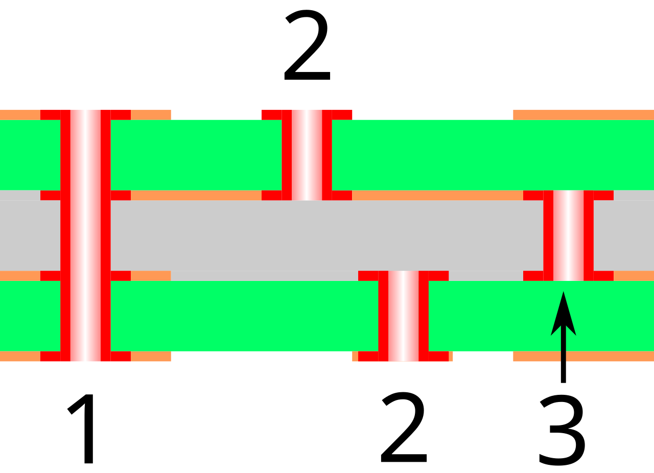
A PCB via (Vertical Interconnect Access) is a plated copper cylinder drilled through the board to connect traces on different layers. Unlike a flat trace, current flows through a thin cylindrical shell of copper — only the plating walls carry current, not the empty drill hole itself.
This means the effective cross-sectional area is much smaller than the drill diameter suggests. A 0.3mm via with 25µm plating has an effective copper cross-section of only about 23,000 mil² — comparable to a very narrow trace. If this area is undersized for the current it carries, the via heats up, the barrel cracks, and the connection fails permanently.
Via Current Formula (IPC-2221 & IPC-2152)
The calculator models the via as a hollow copper cylinder and computes the plating ring cross-section, then applies the IPC thermal formula:
Area = π × ((d/2)² − ((d/2) − t)²)
Imax = k × ΔT0.44 × Area0.725
| Parameter | Symbol | IPC-2221 | IPC-2152 |
|---|---|---|---|
| IPC constant (outer layer via) | k | 0.048 | 0.064 |
| Finished drill diameter | d | User input (mm) | |
| Plating thickness | t | User input (µm → mm) | |
| Allowed temp rise | ΔT | User input (°C) | |
| Class 2 standard plating | — | 20 µm minimum | |
| Class 3 standard plating | — | 25 µm minimum | |
What This Calculator Computes
Max Current — IPC-2221 & IPC-2152 Side by Side
Both standards are shown simultaneously so you can compare the conservative (IPC-2221) and more accurate (IPC-2152) results. IPC-2152 typically rates vias 25–35% higher for the same geometry because it accounts for plane proximity heat-sinking. Use IPC-2221 for most designs; IPC-2152 when optimizing via count in space-constrained layouts.
Via Array — How Many Vias Do You Need?
Enter your required current and the tool calculates the minimum number
of parallel vias needed: N = ⌈I_required / I_max_single⌉.
This is the most common design question for power rails and connector
transitions. The live canvas updates to show the via array footprint
to scale.
Aspect Ratio Check
AR = PCB Thickness / Drill Diameter. The calculator checks
your result against IPC limits automatically:
≤ 10:1 for standard through-hole vias,
≤ 0.75:1 for laser-drilled microvias.
Exceeding the aspect ratio limit means the fabricator cannot reliably plate
the barrel walls, leading to opens and intermittent failures.
Annular Ring DRC
The annular ring is the copper pad remaining around the drill after drilling.
AR = (Pad Diameter − Drill Diameter) / 2.
IPC Class 2 minimum: 0.05mm.
IPC Class 3 minimum: 0.075mm.
The calculator gives a pass/fail against both classes, flagging if
manufacturing tolerances put you at risk of a breakout (drilled hole
touching the pad edge).
Resistance, Voltage Drop & Power Loss
Via resistance: R = ρ × L / A (copper resistivity 1.72×10⁻⁵ Ω·mm).
Voltage drop: V = I × R.
Power loss: P = I² × R.
For a 10A power rail passing through 5 parallel 0.3mm vias,
total via resistance ≈ 1.5 mΩ — a 15mV drop and 150mW heat.
These outputs are essential for power distribution network (PDN) analysis.
Thermal Relief Spoke Bottleneck Audit
Thermal relief spokes are narrower than the full pad and can become the current bottleneck even when the via barrel is adequately sized. Enter spoke count and width and the tool calculates the spokes' current capacity using the same IPC-2221 formula. If the spokes limit below your required current, a ⚠️ bottleneck warning fires and tells you the actual limiting current.
Differential Via Pair Spacing
For high-speed differential pairs (USB, HDMI, PCIe, Ethernet),
the spacing between the two vias in the pair affects differential
impedance. The calculator uses the formula
S = (d/2) × exp(Z_diff × √εr / 120)
to return the optimal center-to-center spacing in mm and mils
for your target impedance and substrate dielectric constant.
Unused Stub Resonance (GHz)
When a via passes through the full board but the signal only uses
part of the barrel, the remaining unused length is a via stub.
Stubs create quarter-wave resonant notches:
f_res = 143 / (4 × L_stub).
Enter the stub length and see the resonant frequency — if it falls
within your signal bandwidth, you have a signal integrity problem
that requires back-drilling to fix.
Via Current Reference Table
| Drill Diameter | Plating (25µm) | Max Current IPC-2221 (10°C) | Max Current IPC-2152 (10°C) | Vias for 5A |
|---|---|---|---|---|
| 0.2mm (8 mil) | 25µm | ~0.35A | ~0.47A | 15 vias |
| 0.3mm (12 mil) | 25µm | ~0.65A | ~0.87A | 8 vias |
| 0.4mm (16 mil) | 25µm | ~0.95A | ~1.27A | 6 vias |
| 0.5mm (20 mil) | 25µm | ~1.25A | ~1.67A | 4 vias |
| 0.6mm (24 mil) | 25µm | ~1.55A | ~2.07A | 4 vias |
| 0.8mm (32 mil) | 25µm | ~2.20A | ~2.93A | 3 vias |
| 1.0mm (40 mil) | 25µm | ~2.90A | ~3.87A | 2 vias |
| 0.3mm (12 mil) | 50µm (filled) | ~1.60A | ~2.13A | 4 vias |
Values are approximate. Always use the calculator above with your exact parameters. Copper-filled vias can carry 2–3× the current of an empty via of the same diameter.
Via Types & When to Use Each
Through-Hole Via
The standard via — drilled all the way through the board from top to bottom. Lowest cost, supports all layer connections. Current capacity is what this calculator primarily models. Aspect ratio limit: 10:1. Use for power connections, ground stitching, and general signal routing.
Blind Via
Connects an outer layer to an inner layer but does not penetrate the full board. More expensive (requires separate drilling and plating steps). Saves space on the opposite side of the board. Common in 4-layer and 6-layer HDI designs. Aspect ratio limit: 0.75:1 for laser-drilled blind microvias.
Buried Via
Connects two inner layers only — invisible from either board surface. Most expensive via type. Used in high-density multilayer designs where surface routing space is exhausted. Requires sequential lamination during fabrication.
Thermal Via
A through-hole or blind via placed directly under a hot component (QFN, MOSFET, LED) to conduct heat through the board to a heat-spreader plane or heatsink. Typically copper-filled or solder-filled for maximum thermal conductivity. Arrays of 4–16 thermal vias are standard under high-power QFN packages.
Design Rules of Thumb
Current & Sizing Rules
- Never rely on a single via for currents above 1A — use 2+ in parallel
- Standard power design: use one 0.3mm via per 0.5A as a safe rule of thumb
- Always keep aspect ratio below 8:1 for reliable plating (10:1 is the absolute limit)
- Apply 20–25% safety margin above the IPC-2221 minimum current
- Use copper-filled vias for high-current paths — doubles current capacity
- Keep via-to-via spacing at least 2× the drill diameter to avoid thermal coupling
High-Speed Signal Rules
- Add return path ground vias adjacent to every signal via transition
- Keep unused stub length as short as possible — back-drill stubs for signals above 3 GHz
- For differential pairs, space the two signal vias symmetrically with equal-sized pads
- Avoid via-in-pad for signals above 10 GHz — the pad capacitance affects impedance
- Use anti-pads (clearance cutouts in planes) to reduce parasitic capacitance
- Place decoupling capacitor vias as close to the power pin as physically possible
Video: PCB Vias 101 — Basics, Sizing & Best Practices
Before sizing your vias, it helps to understand all the via types, how current and thermal limits interact with geometry, and best practices for placement and stitching. Phil's Lab #77 covers all of this in a concise, practical video — directly relevant to using this calculator.
📺 PCB Vias 101 — Basics, Guidelines and Best Practices — Phil's Lab #77. Covers through-hole, blind, buried and microvias, sizing for current and signal integrity, thermal relief, via stitching, and back-drilling. Essential context for understanding every parameter in this calculator.
Frequently Asked Questions — PCB Via Calculator
Common questions about via sizing, IPC standards, aspect ratios, thermal vias, and high-speed design — answered with practical, actionable guidance.
Current & Sizing
How many vias do I need for 5 amps?
With standard 0.3mm vias and 25µm plating at a 10°C temperature rise, each via handles approximately 0.65A (IPC-2221). For 5A you need 8 vias in parallel. With larger 0.6mm vias (~1.55A each), you only need 4. Use the Via Array section of this calculator to find the exact count for your geometry.
Does filling a via with solder increase its current capacity?
Significantly — yes. Solder-filled vias carry approximately 1.5–2× the current of an empty via of the same diameter because the solder increases the effective cross-section carrying current. Copper-filled vias (specified at fab time) carry up to 3× more due to copper's higher conductivity vs. solder. EEVblog #543 tested this empirically and confirmed the improvement.
How does plating thickness affect via current capacity?
Plating thickness directly determines the copper cross-sectional area. Doubling plating from 20µm to 40µm does not double current capacity — the IPC formula's 0.725 exponent gives roughly a 60–70% increase. IPC Class 2 specifies 20µm minimum plating; Class 3 specifies 25µm. Premium fabricators offer 35µm (equivalent to 1oz copper thickness) for high-current applications.
Can I use via stitching for high-current power rails?
Yes — via stitching (placing an array of vias) is the standard method for transitioning high-current connections between layers. The total current capacity equals the single-via rating multiplied by the number of vias, assuming the current splits evenly. Always route with a star topology from the via array to the load for even current sharing.
Design Rules & Standards
What is via aspect ratio and what is the safe limit?
Aspect ratio = board thickness ÷ drill diameter. Most standard fabricators require below 10:1 for reliable plating. For a standard 1.6mm board, minimum via diameter is 0.16mm. High-density boards often target 8:1 maximum. Laser-drilled microvias have a much stricter limit: 0.75:1 for single stack and 1:1 for stacked microvias.
What is an annular ring and when does it fail?
The annular ring is the copper pad area remaining after drilling. If the drill wanders during fabrication (drill wander tolerance is typically ±0.05–0.1mm), a small annular ring can result in the drill breaking through the pad edge — called a breakout, which destroys the via. IPC Class 2 requires minimum 0.05mm ring; Class 3 requires 0.075mm. Design with at least 0.15mm for safety.
What is the difference between Class 2 and Class 3 plating?
IPC Class 2 (general commercial) requires a minimum plating thickness of 20µm. IPC Class 3 (high reliability — medical, military, aerospace) requires 25µm minimum. Class 3 boards are more expensive to fabricate and have tighter tolerances throughout. Most consumer and industrial electronics use Class 2.
Should I tent (mask) my vias?
Tenting prevents solder wicking into the via during assembly and protects the barrel from oxidation. Tent all signal vias by default. Leave thermal vias open or have them copper/epoxy-filled if they sit under component pads. Never tent via-in-pad designs without first specifying copper fill — untented via-in-pad causes solder voiding under the component.
What is back-drilling and when is it needed?
Back-drilling (controlled-depth drilling from the back of the board) physically removes the unused via stub, eliminating stub resonance entirely. It is required for signals above 3–5 GHz and for PCIe Gen 4/5, 25G+ Ethernet, and other high-speed serial links. Back-drilling adds cost and requires tight depth control (typically ±0.05–0.1mm) from the fabricator.
How do thermal vias work for heat dissipation?
Thermal vias conduct heat vertically through the board via copper's high thermal conductivity (385 W/m·K vs. FR-4's 0.3 W/m·K). An array of 9–16 copper-filled 0.3mm vias under a QFN package provides a thermal resistance of approximately 5–15°C/W to a bottom-side copper plane — enough for components dissipating 1–5W. The vias must be copper or silver-epoxy filled; air-filled vias have significantly higher thermal resistance.
Advanced PCB Via Design Concepts
Via Inductance at High Frequencies
At GHz frequencies, a via is not just a conductor — it is an inductor.
Via inductance is approximately:
L_via ≈ (µ₀ × h / 2π) × ln(4h/d)
For a 1.6mm via of 0.3mm diameter, L_via ≈ 0.8 nH.
At 5 GHz, this represents an impedance of ~25Ω — significant compared
to the 50Ω trace impedance. This inductance, combined with pad capacitance,
creates an LC resonance that must be considered for signals above 1 GHz.
The via stub resonance feature in this calculator is the most visible
manifestation of this effect.
Return Path Vias — Why Every Signal Via Needs a Ground Via
When a high-speed signal transitions between layers via a via, its return current (flowing in the ground plane) must also transition. If there is no nearby ground via, the return current takes a long, indirect path — creating a current loop that radiates EMI and increases impedance discontinuity. Best practice: place a ground via within 1× the via drill diameter of every signal via, on the same side as the signal pad. For differential pairs, place two ground vias flanking the pair symmetrically.
Via-in-Pad Design Considerations
Via-in-pad (placing a via directly in a component pad) is used in HDI designs to reduce inductance and save routing space under fine-pitch BGAs and QFNs. Critical requirements:
- The via must be copper or epoxy filled and planarized — an open via-in-pad causes solder to wick away from the component during reflow
- Specify this as a fabrication note: "Via-in-pad, copper filled, planarized"
- Increases fabrication cost by approximately 20–40%
- Benefits: lower inductance, better thermal performance, reduced BGA ball voiding
IPC-2221 vs IPC-2152 — The Practical Difference for Vias
For a 0.3mm via with 25µm plating at 10°C rise: IPC-2221 gives ~0.65A, IPC-2152 gives ~0.87A — a 34% difference. This matters when designing via arrays: IPC-2221 says you need 8 vias for 5A; IPC-2152 says 6 vias. Two fewer vias per power connection multiplied across a complex design can save significant board area. However, IPC-2152's higher rating assumes the via is near a copper plane — an isolated via in a signal layer may be closer to the IPC-2221 figure.
Related Free Tools on CircuitsLab Wiki
- PCB Trace Width Calculator — IPC-2221 & IPC-2152 trace current capacity, DCR, voltage drop
- Planar Inductor Calculator — PCB spiral coil inductance, Q-factor, SRF
- Skin Depth Calculator — AC copper resistance at RF frequencies
- Resistor Color Code Calculator — 4-band and 5-band resistor decoding
- LED Series Resistor Calculator — Safe current limiting for LEDs
- Digital Logic Simulator — Browser-based logic gate and flip-flop simulator